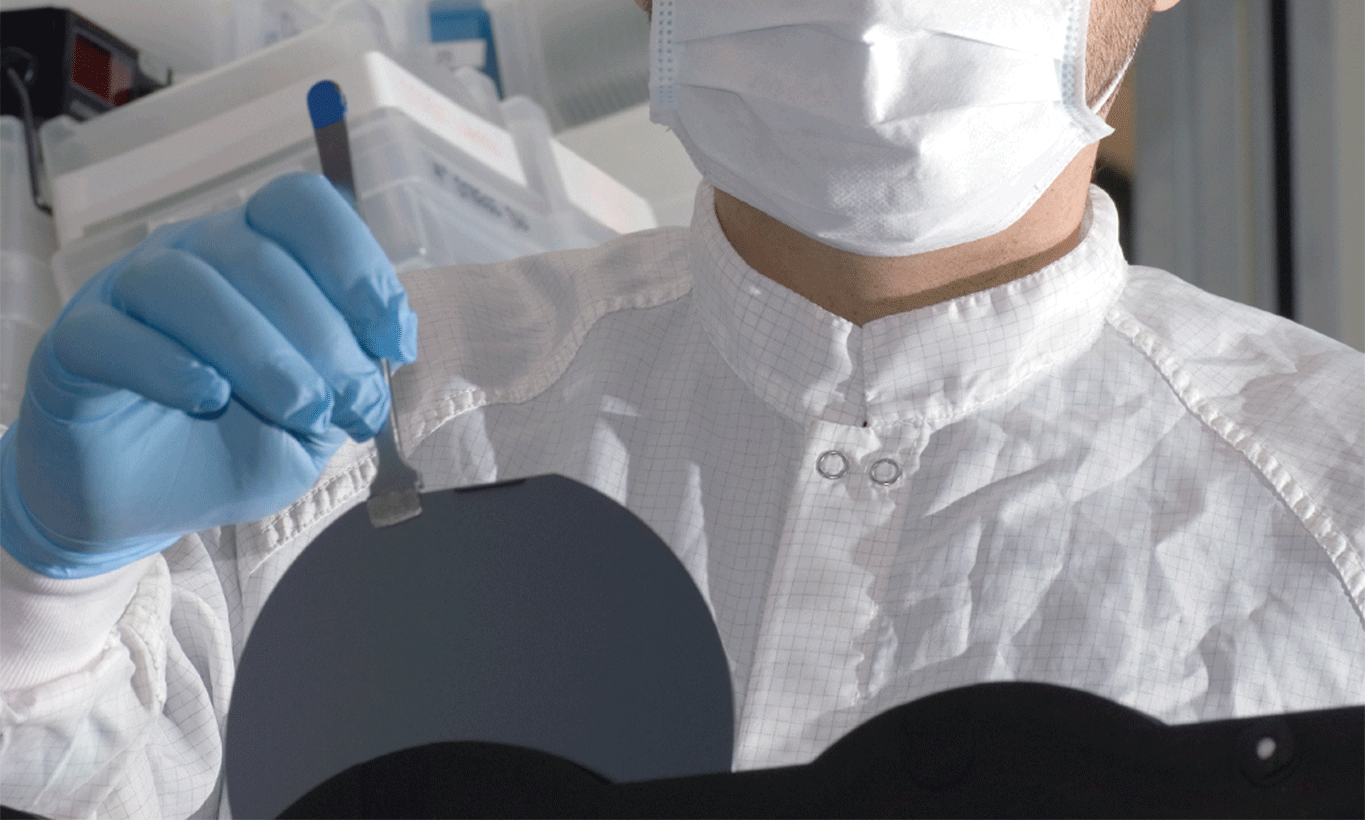
Processing Fused Wafers
Learn Logitech process routes for thinning down the top wafer of a two wafer fusion bonded assembly.
With over 50 years experience in the production of lapping & polishing systems for wafer processing, Logitech has responded to the need for successful methods of fused wafer thinning.
Learn the process:
Download the application note on "Fused Wafers" to learn the process routes and methodologies to achieve a final thickness as low as 10μm.
You'll also benefit from insight on:
- Temporary bonding that minimises risk of breakage whilst maintaining sample yield
- Intelligent features for automated processing operations with minimal user input
- Two-in-one systems for first phase thinning and subsequent polishing
Embrace the cutting edge – you’re in safe hands.

