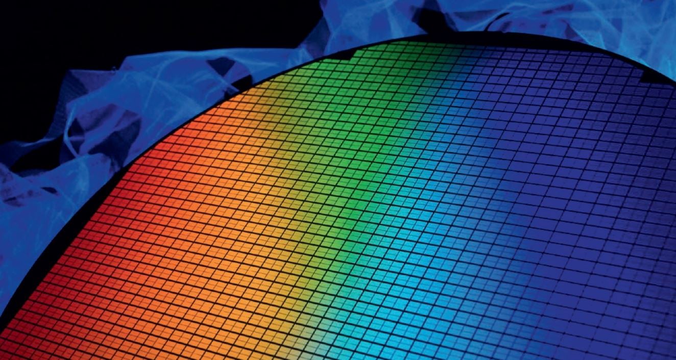
4” GaAs Wafer Backthinning
Discover why GaAs wafers are the becoming the worldwide semiconductor material of choice.
A variety of different wafer materials and sizes are used across the semiconductor industry. GaAs (Gallium Arsenide) wafers exhibit certain electronic properties that are superior to Silicon (Si). This advantage has allowed GaAs wafers to become popular in high frequency and opto-electronic applications, despite strict industry requirements.
Learn the process:
Download the application note to obtain process requirements, methodologies and system specifications required in order to process GaAs to its optimum geometric control.
Download the free application note for information achieving:
- Surface roughness: < mnm Ra over a 2mm dektak trace.
- Flatness: +/-2 microns over a 100mm (4") diameter wafer.
- Thickness uniformity (TTV): +/-2 microns over a 100mm (4") diameter wafer.
Embracing the cutting edge – you’re in safe hands.

